GT New Horizons · Ultimate Voltage (UV)
PCB Factory
The PCB Factory is a UV tier multiblock for crafting circuit boards much more efficiently than the Large Chemical Reactor. Not only does it become a one-step process, but it uses significantly less resources for wetware and bioware circuit boards. The PCB Factory is also the only machine capable of manufacturing optical circuit boards which are mandatory for progression in UEV. The gate to building the PCB Factory is a single wetware circuit board for the data stick.
The Bio Chamber and Cooling Tower are two additional structures or upgrades that can be built around the PCB Factory to improve its functionality. The Bio Chamber unlocks the recipes for wetware and bioware circuit boards and the Cooling Tower unlocks either imperfect or perfect overclocks depending on the tier of the structure and the coolant provided. The upgrades must be built within 16 blocks of the PCB Factory's controller and are linked with a data stick, similar to the Waterline multiblocks.
Construction
The PCB Factory is available in three tiers but they all share the same controller. The T2 structure adds some photolithographic framework casings to the T1 structure, but the T3 structure is completely different. The glass can be any tier and has no effect on the operation of the machine. Multi-amp and laser energy hatches are supported for serious overclocking. Use the Multiblock Structure Hologram Projector to visualize/build the structure with subchannel "glass" to specify the tier of the glass and the projector stack size to specify the structure tier.
The nanite containment bus is effectively an input bus exclusively for nanites. The maximum capacity is 2,048 but the maximum number of parallels is reached with only 1,618 nanites. The T1 structure does not require one because it does not use nanites.
| T1 PCB Factory
Unlocks T1 recipes
|
T2 PCB Factory (Adds to T1)
Unlocks T2 recipes and parallels with silver nanites
|
T3 PCB Factory (New Structure)
Unlocks T3 recipes and parallels with gold nanites
|
There are also two additional structures or upgrades that can be built around the PCB Factory to improve its functionality at the cost of power. Both upgrades have their own controller and therefore can be built with the Multiblock Structure Hologram Projector. Their exact position and orientation does not matter as long as their controllers are within 16 blocks of the PCB Factory's controller. Link structures by first left-clicking the PCB Factory controller with a data stick and then right-clicking the upgrade(s) within range. Multiple PCB Factories can link to the same upgrade(s) to share them. The power consumption of each PCB Factory increases by the square root of the number of upgrades, which means one upgrade multiplies the power consumption by x1.00 (does nothing) and two upgrades multiplies the power consumption by x1.41.
One T2 Cooling Tower requires 70.0k (L) infinity, 55.3k (L) spacetime, and 13.8k (L) hypogen to build. The perfect overclocks of the T2 Cooling Tower are extremely powerful and allow players to craft a limitless number of circuit boards with only one or two PCB Factories, even in the end game.
| Bio Chamber
Unlocks the recipes for wetware and bioware circuit boards
|
T1 Cooling Tower
Unlocks imperfect overclocks (2/4) at the cost of 10 L/s of distilled water while running
|
T2 Cooling Tower (New Structure)
Unlocks perfect overclocks (4/4) at the cost of 10 L/s of super coolant while running
|
-
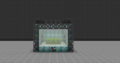 1) T1 PCB Factory
-
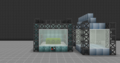 2) T1 PCB Factory with Bio Chamber
-
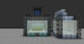 3) T1 PCB Factory with Bio Chamber and T1 Cooling Tower
-
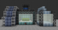 4) T2 PCB Factory with Bio Chamber and T1 Cooling Tower
-
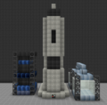 5) T3 PCB Factory with Bio Chamber and T1 Cooling Tower
-
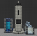 6) T3 PCB Factory with Bio Chamber and T2 Cooling Tower
-
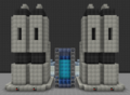 7) T3 PCB Factory with shared Bio Chambers and T2 Cooling Tower
Wallsharing
PCB Factories may wallshare the entire T2 addition which means a single set of reinforced photolithographic framework casings is enough to upgrade two machines at once. The additional structures or upgrades are also shareable between PCB Factories--simply link them to more than one within range. The T3 PCB Factory can even overlap enough to share buses/hatches, including the nanite containment bus.
Usage
Trace Size
Trace size refers to the width of the lines transmitting electrical signals between components on the circuit board. Trace size can either be lowered to slow down the machine and produce more boards from the same amount of resources, or increased to make the machine run faster and produce fewer boards. The input amounts never change. Trace Size can only be between 50-200 μm, but the most common is 50.
|
| ||||||||||||||
Nanites
T2 recipes require at least one silver nanite and T3 recipes require at least one gold nanite. Additional nanites increases the number of parallels that the machine can run, as seen in the following table/equation. The ceiling operator rounds any decimal values up to the next whole number. The absolute maximum number of parallels is 256. Nanites from other tiers have no effect (ie. silver nanites do nothing in a T3 PCB Factory). Craft nanites in a Nano Forge and place them in the nanite containment bus, NOT an input bus or crafting input buffer.
|